


イオンコーター Ion Coater
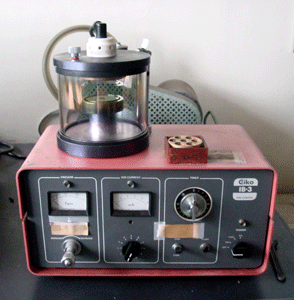
走査型電子顕微鏡用試料の導体化コーティングを行なう装置です。
真空中で気体放電を起こさせると、正に帯電した気体イオンが固体に衝突して構成原子が叩きだされます。この現象をイオンスパッタリングと呼びます。そこで、負電極に導体化コーティング金属を用いると、金属原子が叩きだされて試料に均一な薄膜を形成します。
Ion coater is a device for conductive coating for SEM samples.
When a gas discharge occurs in a vacuum, positively charged gas ions collide with a solid and knock out its constituent atoms. This phenomenon is called ion sputtering. When a conductive coated metal is used as the negative electrode, the metal atoms are knocked out to form a uniform thin film on the sample.
設置機器メーカー/型式 Equipment
エイコー精機製/IB-3(Eiko Seiki/IB-3)
仕 様 Specs
試料台 52ミリ径
イオン化電圧 DC 0 〜 1400 V
イオン化電流 10 mA
Sample stage diameter: 52 mm
Ionization voltage: DC 0 〜 1400 V
Ionization current: 10 mA
設置場所 Location
4階 顕微鏡標本作製室1(405号室)
Microscopy Sample Preparation Room #1 (Room #405, CRL 4th floor)
担当者 Contact person
山元 武文(Takefumi Yamamoto)(TEL 2304)
福永 祥子(Sachiko Fukunaga)(TEL 2303)
岡本 久美(Kumi Okamoto)(TEL 2302)学内向け SUMS only
|
|
先頭へ TOP |
Last Updated 2022/11/08